My 8-bit CPU
My goals for this project
Create a Turing-Complete CPU
After the completion of the project, I wanted to create a programmable Turing-complete CPU.
Learn CPU Architecture
Through research and practice, I wanted to become familiar with the role of every component in a standard CPU.
Work with Assembly
Learn Assembly, one of the lowest levels of computing. This is essential to interface with the CPU’s machine code.
Practice Breadboarding
Such a large breadboard project requires knowledge of proper breadboarding techniques to even consider building.
Learn Cad (in-progress)
I need to make schematics of this project to convert everything to PCB in the future.
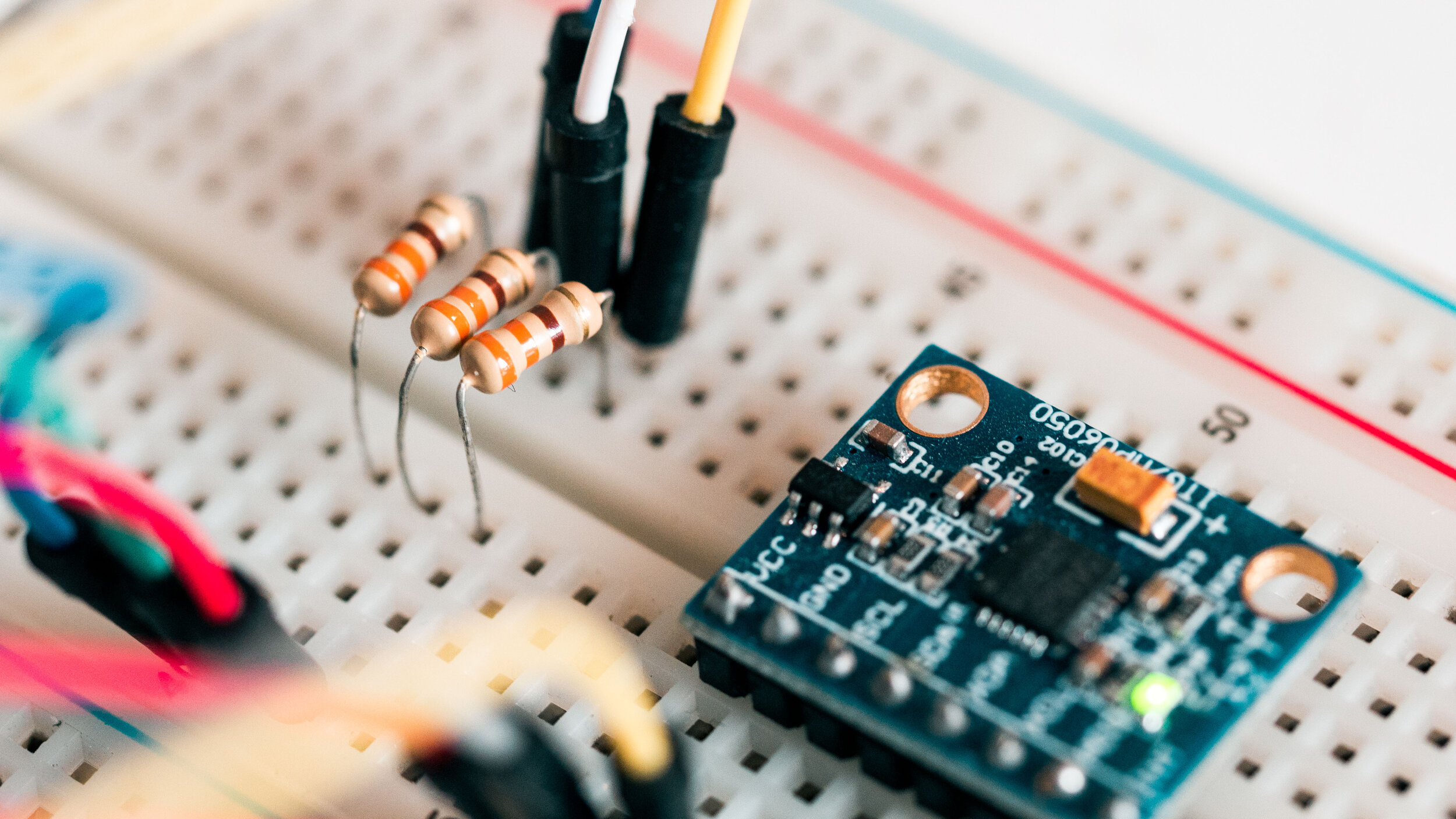
Components (placeholder pictures)

1 KHz Clock
The CPU Clock is essential for the cooperation between the different components of the CPU. Each clock pulse triggers another cycle where information transfer occurs between the components, enabling the execution of instructions. The clock speed determines how fast these pulses occur.
In some of the fastest CPUs available on the market, clock speeds can hit upwards of 4+ billion pules per second (4+ GHz) — about 4 million times faster than my 8-bit CPU.

Bus
The bus is a centralized connection between all the components. Only one component can write to the bus per clock cycle, but multiple components can read the value on the bus.
The bus on my 8-bit CPU is 8-bits wide similar to the earliest ISA models.

1KB RAM
Random Access Memory (RAM) is the main component that stores data. Programs are loaded into RAM and then interpreted and executed by the CPU. There are several data structures within RAM, most notably heap and stack, but my build only supports heap.
In my 8-bit CPU, the 1KB RAM is split into 4 pages of 256 bytes of RAM. Here, each page represents a different program that is stored within the RAM. The selected program is displayed in binary by LEDs.

Program Counter
The program counter has the sole purpose of keeping track of the memory address of the next instruction. After each instruction, the CPU fetches the instruction at the address specified by the program counter.

ALU
The Arithmetic Logic Unit (ALU) is the only part of the CPU that does the actual computing.
The operations the ALU can do determines what calculations the CPU can do. Some of the most common operations include:
bitwise OR/AND/XOR/NOT
bitwise shift left/right (circular as well)
Addition/Subtraction
These operations can be then combined in instructions to do more complex tasks like multiplication, division, and comparisons.
My implementation of the ALU has these operations
Addition/Subtraction

Registers
Registers temporarily store a single value within them. They are typically split into two categories:
General Purpose Registers
Special Purpose Registers
The only difference between these is that special purpose registers also serve another function besides just storing a value. See the section about the registers below for more details.

7-Segment Display
The seven segment display is attached to a Register O (a special purpose register) and displays the contents of it in either unsigned decimal (0 to 255) or two’s complement decimal (-128 to 127).

LCD Screen
The LCD acts as a write-only special purpose register. It can display any UTF-8 character and can interpret instructions for itself as well (move the cursor, clear the screen, etc).
In essence, there is a microcontroller that interfaces with the actual screen and does all the work of displaying text.

The Pre-Build
Before I build, I need to know what to build.
//TODO: make this stuff

The Build
Time to finally build everything.
//TODO: make this stuff

The Debugging
The longest part
//TODO: make this stuff

The Finished Product
After months of work…
//TODO: Pictures.
Schematics
Cad schematics coming soon